- 您现在的位置:买卖IC网 > Sheet目录1992 > CY28551LFXC-3T (Silicon Laboratories Inc)IC CLOCK INTEL/AMD SIS VIA 56QFN
CY28551-3
....................Document #: 001-05677 Rev. *D Page 26 of 28
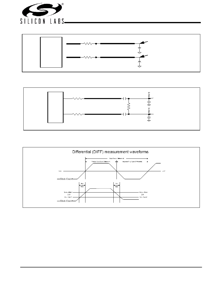
The following diagrams show the test load configuration for the differential CPU and PCIEX outputs.
22
M e asurem en t
Po in t
2 pF
50
22
M e asurem en t
Po in t
2 pF
50
L 1
L 2
L 1
L 2
L 1 = 0.5" , L 2 = 7 "
OU T +
OU T -
Figure 14. Differential Load Configuration for 0.7 Push Pull Clock
CP UT _ K 8
TPC B
CP UC_ K 8
15 O h m
39 00 pF
L1
L2
L3
L1
L2
L3
T PC B
39 00 pF
1 69 O h m
M e a s ur em en t
Po i n t
M e as ur em en t
Po i n t
5 pF
5 p F
12 5 O h m
1. 25V
1. 2 5 V
12 5 O h m
Figure 15. Differential Load Configuration for 3.3 Push Pull Clock
Figure 16. Differential Measurement for Differential Output Signals (for AC Parameters Measurement)
发布紧急采购,3分钟左右您将得到回复。
相关PDF资料
CY28551LFXC
IC CLOCK INTEL/AMD SIS VIA 64QFN
CY2SSTV855ZXI
IC CLOCK DIFFDRV PLL DDR 28TSSOP
CY2SSTV857ZXI-27
IC CLK DDR266/333BUF1:10 48TSSOP
CY2SSTV857ZXI-32
IC CLK DDR266/333BUF1:10 48TSSOP
CY505YC64DT
IC CLK CK505 BROADWATER 64TSSOP
CYW150OXC
IC CLOCK 440BX AGP 56SSOP
CYW173SXC
IC CLK GEN TAPE DRV 4CH 16SOIC
CYW305OXC
IC CLOCK W305 SOLANO 56SSOP
相关代理商/技术参数
CY28551LFXCT
功能描述:时钟发生器及支持产品 Universal System Clk Intel AMD SiS Via RoHS:否 制造商:Silicon Labs 类型:Clock Generators 最大输入频率:14.318 MHz 最大输出频率:166 MHz 输出端数量:16 占空比 - 最大:55 % 工作电源电压:3.3 V 工作电源电流:1 mA 最大工作温度:+ 85 C 安装风格:SMD/SMT 封装 / 箱体:QFN-56
CY2862-000
制造商:TE Connectivity 功能描述:82A0111-4-9-G110
CY2863-000
制造商:TE Connectivity 功能描述:82A0111-8-9-G110 - Bulk
CY28800
制造商:CYPRESS 制造商全称:Cypress Semiconductor 功能描述:100-MHz Differential Buffer for PCI Express and SATA
CY28800OXC
功能描述:时钟缓冲器 PCI Express & Sata Diff Buffer 100MHz RoHS:否 制造商:Texas Instruments 输出端数量:5 最大输入频率:40 MHz 传播延迟(最大值): 电源电压-最大:3.45 V 电源电压-最小:2.375 V 最大功率耗散: 最大工作温度:+ 85 C 最小工作温度:- 40 C 封装 / 箱体:LLP-24 封装:Reel
CY28800OXCT
功能描述:时钟缓冲器 PCI Express & Sata Diff Buffer 100MHz RoHS:否 制造商:Texas Instruments 输出端数量:5 最大输入频率:40 MHz 传播延迟(最大值): 电源电压-最大:3.45 V 电源电压-最小:2.375 V 最大功率耗散: 最大工作温度:+ 85 C 最小工作温度:- 40 C 封装 / 箱体:LLP-24 封装:Reel
CY28800OXI
功能描述:时钟缓冲器 PCI Express & Sata Diff Buffer 100MHz RoHS:否 制造商:Texas Instruments 输出端数量:5 最大输入频率:40 MHz 传播延迟(最大值): 电源电压-最大:3.45 V 电源电压-最小:2.375 V 最大功率耗散: 最大工作温度:+ 85 C 最小工作温度:- 40 C 封装 / 箱体:LLP-24 封装:Reel
CY28800OXIT
功能描述:时钟缓冲器 PCI Express & Sata Diff Buffer 100MHz RoHS:否 制造商:Texas Instruments 输出端数量:5 最大输入频率:40 MHz 传播延迟(最大值): 电源电压-最大:3.45 V 电源电压-最小:2.375 V 最大功率耗散: 最大工作温度:+ 85 C 最小工作温度:- 40 C 封装 / 箱体:LLP-24 封装:Reel